China has quietly developed an early prototype of an extreme ultraviolet (EUV) lithography system, a breakthrough technology that sits at the heart of the world’s most advanced semiconductor manufacturing. The development marks a significant milestone in Beijing’s long-running effort to reduce reliance on foreign chipmaking tools that are currently restricted by the United States and its allies.
According to a report by Reuters, scientists working inside a high-security research facility in Shenzhen completed the prototype in early 2025. The project reportedly brought together a tightly coordinated network of Chinese research institutes, domestic suppliers, and engineers, including individuals with prior experience at ASML, the Dutch company that currently holds a global monopoly on EUV lithography systems.
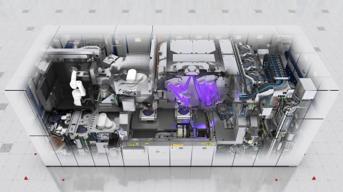
The prototype is capable of generating extreme ultraviolet light, a critical requirement for producing cutting-edge chips at advanced process nodes. While this achievement represents a major technical step forward, the system remains in the testing phase and has not yet been used to manufacture functional semiconductor chips. Sources familiar with the project suggest that realistic timelines for working chips produced using the technology range between 2028 and 2030.
Significant engineering challenges remain. EUV lithography demands extraordinary precision in optics, vibration control, and system reliability. These are areas in which ASML invested decades of research and refinement before achieving commercial-scale success. Replicating that level of performance, consistency, and yield remains a formidable task for any newcomer.
At present, ASML is the only company in the world capable of supplying EUV tools for high-volume chip manufacturing. Each system costs approximately $250 million and is essential for producing the most advanced chips designed by companies such as NVIDIA and AMD, and manufactured by leading foundries including TSMC, Intel, and Samsung.
Reuters describes China’s effort as the culmination of a roughly six-year, state-backed initiative aimed at achieving technological self-sufficiency in semiconductors. People close to the project have compared it to a Chinese-scale “Manhattan Project,” underscoring both the strategic importance and the massive resources involved.
Despite the progress, experts caution that large-scale chip production using China’s EUV system is still years away rather than imminent. Even so, the prototype signals a meaningful shift in the global semiconductor landscape, highlighting China’s determination to overcome export controls and compete at the highest levels of chip manufacturing technology.