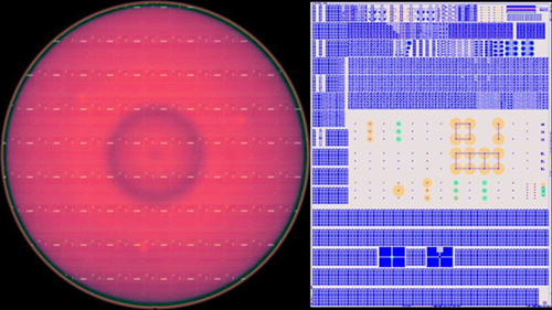
In a groundbreaking advancement for semiconductor technology, IMEC, the world-leading research and innovation hub in nanoelectronics, has achieved a world-record gallium nitride (GaN) breakdown voltage exceeding 650 volts on a 300-mm QST™ substrate developed by Shin-Etsu Chemical Co., Ltd.
This achievement marks a major leap in power electronics, setting a new global standard for high-efficiency, high-performance GaN-on-silicon technology — a key enabler for the next generation of electric vehicles (EVs), renewable energy systems, and data centers.
IMEC’s latest research demonstrates the successful integration of GaN (Gallium Nitride) on Shin-Etsu’s QST™ (Quartz Substrate Technology), achieving a record breakdown voltage above 650 V while maintaining low leakage current and high thermal stability.
This breakthrough overcomes one of the biggest challenges in GaN-on-Si technology — the stress and lattice mismatch that limit performance and reliability at higher voltages. The QST™ substrate’s unique design provides superior mechanical strength and heat dissipation, making it ideal for large wafer (300 mm) GaN power devices.
Gallium Nitride is already revolutionizing the power electronics industry, enabling smaller, faster, and more energy-efficient components. However, scaling GaN to 300 mm wafers with high breakdown voltages has long been a technological barrier.
IMEC’s record-breaking result now opens the door for mass manufacturing of high-voltage GaN power devices that can outperform traditional silicon-based components in key sectors like:
Electric vehicles (EV fast chargers & onboard converters)
5G power amplifiers
Renewable energy systems (solar inverters, wind turbines)
High-efficiency data center power supplies
Industry Impact & Collaboration
This achievement was made possible through close collaboration between IMEC and Shin-Etsu Chemical, combining IMEC’s decades of GaN research expertise with Shin-Etsu’s advanced materials innovation.
Dr. Marian Verhelst, IMEC’s VP of Semiconductor Research, stated:
“This record-setting result underscores IMEC’s leadership in GaN power technology and validates the scalability of our process for next-generation 300-mm wafer platforms. It’s a key step toward the widespread commercialization of GaN power devices.”
Shin-Etsu Chemical added that its QST™ substrate not only improves reliability but also reduces wafer bowing — a critical advantage for high-volume semiconductor manufacturing.
With this new record, IMEC reinforces its position at the forefront of sustainable, energy-efficient semiconductor innovation. The ability to produce high-voltage, high-yield GaN devices on large wafers could drastically cut production costs and carbon footprints for the electronics industry worldwide.